Journals > > Topics > Special Issue for Ultrafast Laser Precision Machining of Hard and Brittle Materials
Special Issue for Ultrafast Laser Precision Machining of Hard and Brittle Materials|12 Article(s)
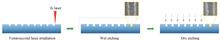
Fabrication of Sapphire Grating by Femtosecond Laser Assisted Etching(Invited)
Jiaxin ZHENG, Bingrong GAO, Yafei XUE, Ziyi LUO, Shanguo HAN, Xueqing LIU, and Qidai CHEN
By using femtosecond laser assisted etching technology, a grating structure with adjustable period, duty cycle and height is achieved on sapphire surface. It solves the problem of poor surface quality in femtosecond laser processing of hard and brittle materials, such as low processing accuracy caused by debris accumulation, and difficulty in preparing deep structures. The roughness of the sapphire grating structure was reduced from 78 nm (after direct laser writing) to 7 nm (after dry etching), and the sapphire microstructures with a period of 800 nm and a aspect ratio of 4 were fabricated. The femtosecond laser assisted etching technology can prepare a high smoothness grating on sapphire surface, and the result proves that this technology can significantly improve the diffraction efficiency of each diffraction order. By using femtosecond laser assisted etching technology, a grating structure with adjustable period, duty cycle and height is achieved on sapphire surface. It solves the problem of poor surface quality in femtosecond laser processing of hard and brittle materials, such as low processing accuracy caused by debris accumulation, and difficulty in preparing deep structures. The roughness of the sapphire grating structure was reduced from 78 nm (after direct laser writing) to 7 nm (after dry etching), and the sapphire microstructures with a period of 800 nm and a aspect ratio of 4 were fabricated. The femtosecond laser assisted etching technology can prepare a high smoothness grating on sapphire surface, and the result proves that this technology can significantly improve the diffraction efficiency of each diffraction order.
Acta Photonica Sinica
- Publication Date: Jun. 25, 2021
- Vol. 50, Issue 6, 84 (2021)


Influence of Laser Pulse Width on the Performance of Glass Waveguide(Invited)
Yingde WANG, Yanhao YU, Zhennan TIAN, and Qidai CHEN
By changing the laser pulse width, the optical waveguide is directly written in boro-aluminosilicate glass, and the effects of the pulse width on the section morphology of the optical waveguide, the size of the mode field and the transmission ratio of the directional coupler are studied. In the experiment, a single mode/multi-mode critical power laser with a pulse width of 239 fs is used to fabricate the waveguide. The cross section size of the waveguide changes from 5.4 μm×4.2 μm (239 fs) to 5.1 μm×2.4 μm (700 fs). The size of the mode field changed from 6.2 μm×6 μm (239 fs) to 5.8 μm×4.8 μm(700 fs) and the transmission modes were single mode. The shape of the mode field gradually changed from round to ellipse. The transmission ratio of the directional coupler changes from 97.8% (239 fs) to 70.2% (700 fs) in the horizontal polarization and from 99.2% (239 fs) to 79.7% (700 fs) in the vertical polarization. Experiments have found that the laser with a pulse width of more than 600fs is not conducive to the preparation of waveguides with stable performance. By changing the laser pulse width, the optical waveguide is directly written in boro-aluminosilicate glass, and the effects of the pulse width on the section morphology of the optical waveguide, the size of the mode field and the transmission ratio of the directional coupler are studied. In the experiment, a single mode/multi-mode critical power laser with a pulse width of 239 fs is used to fabricate the waveguide. The cross section size of the waveguide changes from 5.4 μm×4.2 μm (239 fs) to 5.1 μm×2.4 μm (700 fs). The size of the mode field changed from 6.2 μm×6 μm (239 fs) to 5.8 μm×4.8 μm(700 fs) and the transmission modes were single mode. The shape of the mode field gradually changed from round to ellipse. The transmission ratio of the directional coupler changes from 97.8% (239 fs) to 70.2% (700 fs) in the horizontal polarization and from 99.2% (239 fs) to 79.7% (700 fs) in the vertical polarization. Experiments have found that the laser with a pulse width of more than 600fs is not conducive to the preparation of waveguides with stable performance.
Acta Photonica Sinica
- Publication Date: Jun. 25, 2021
- Vol. 50, Issue 6, 78 (2021)
Fabrication of High Temperature Resistant Geometric Phase Element Inside Sapphire by Femtoesecond Laser(Invited)
Yiming LU, Bingrong GAO, Xueqing LIU, and Qidai CHEN
Aiming at the problems of difficult processing, low precision and poor effect of fabricating geometric phase elements in crystal materials, a femtosecond laser-induced nano-grating technology was proposed to fabricate the internal geometric phase diffraction elements. The femtosecond laser near-threshold processing method effectively improves the processing accuracy and the fabricating accuracy is 340 nm. By adjusting the polarization of the scanning laser, the direction of the induced nano-grating can be accurately controlled, leading to the change of the slow axis direction of the crystalline birefringence. Based on this method, the geometric phase Fresnel zone plate in sapphire has been fabricated. The device has a good morphology with no cracks and excellent optical performance, which can be used for focusing in high-temperature environments. Aiming at the problems of difficult processing, low precision and poor effect of fabricating geometric phase elements in crystal materials, a femtosecond laser-induced nano-grating technology was proposed to fabricate the internal geometric phase diffraction elements. The femtosecond laser near-threshold processing method effectively improves the processing accuracy and the fabricating accuracy is 340 nm. By adjusting the polarization of the scanning laser, the direction of the induced nano-grating can be accurately controlled, leading to the change of the slow axis direction of the crystalline birefringence. Based on this method, the geometric phase Fresnel zone plate in sapphire has been fabricated. The device has a good morphology with no cracks and excellent optical performance, which can be used for focusing in high-temperature environments.
Acta Photonica Sinica
- Publication Date: Jun. 25, 2021
- Vol. 50, Issue 6, 71 (2021)
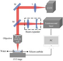
Water-assisted Femtosecond Laser Silicon Carbide Micro-hole Machining(Invited)
Sijia XU, Yanhao YU, and Qidai CHEN
A water-assisted femtosecond laser silicon carbide micro-hole machining method is proposed, and a 200 μm diameter micro-hole is processed on a 350 μm thick silicon carbide sample. The difference between processing micro-holes in air and water-assisted processing of micro-holes is discussed. Water reduces the temperature of the processing area, greatly reducing the occurrence of oxidation reactions. The debris produced by processing is taken away by the water, avoiding the formation of HAZ and reducing the roughness of the sample. The processed micro-holes have smooth sidewalls and no HAZ, which has practical application value in industry. The processing method makes it a reality to process silicon carbide micropores with good morphology, and is expected to be applied to the industrial processing of silicon carbide. A water-assisted femtosecond laser silicon carbide micro-hole machining method is proposed, and a 200 μm diameter micro-hole is processed on a 350 μm thick silicon carbide sample. The difference between processing micro-holes in air and water-assisted processing of micro-holes is discussed. Water reduces the temperature of the processing area, greatly reducing the occurrence of oxidation reactions. The debris produced by processing is taken away by the water, avoiding the formation of HAZ and reducing the roughness of the sample. The processed micro-holes have smooth sidewalls and no HAZ, which has practical application value in industry. The processing method makes it a reality to process silicon carbide micropores with good morphology, and is expected to be applied to the industrial processing of silicon carbide.
Acta Photonica Sinica
- Publication Date: Jun. 25, 2021
- Vol. 50, Issue 6, 66 (2021)
Fabrication of Time Capsules by Femtosecond Laser-induced Birefringence(Invited)
Lin WANG, Hua FAN, Zhenze LI, Yi WANG, Yishi XU, Lei WANG, and Qidai CHEN
Femtosecond laser-induced birefringent voxels were explored by using birefringent microscope and optical microscope. It shows that the retardance increases as the pulse number increases. Two types of structures are found. Type X structures require at least 20 pulses and single pulse energy no more than 854 nJ. More, the pulse duration must limited between 300 fs and 600 fs. Additionally, the data storage process is presented by taking Chinese characters of "Acta Photonica Sinica" as example. Time capsules containing the history of Jilin Province, the history of Jilin University, and the history of Tsinghua University are prepared. Femtosecond laser-induced birefringent voxels were explored by using birefringent microscope and optical microscope. It shows that the retardance increases as the pulse number increases. Two types of structures are found. Type X structures require at least 20 pulses and single pulse energy no more than 854 nJ. More, the pulse duration must limited between 300 fs and 600 fs. Additionally, the data storage process is presented by taking Chinese characters of "Acta Photonica Sinica" as example. Time capsules containing the history of Jilin Province, the history of Jilin University, and the history of Tsinghua University are prepared.
Acta Photonica Sinica
- Publication Date: Jun. 25, 2021
- Vol. 50, Issue 6, 58 (2021)

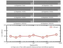
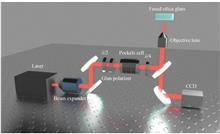
Temporal-spatial Dynamics of Femtosecond Time Resolved Plasma in Femtosecond Laser Induced Microstructure(Invited)
Fengqin HUANG, Tianlun SHEN, Jinhai SI, Tao CHEN, and Xun HOU
Temporal-spatial evolutions of transient plasma in single pulse femtosecond (fs) laser induced microstructure in fused silica were investigated using fs time-resolved pump-probe shadowgraphy. The relation between the spatial distribution of transient electron density and the distribution of fs laser-induced microstructure in fused silica were also studied. In this study, the fs laser was focused by two kinds of microscope objectives with different Numerical Aperture (NA). The results showed that the transient peak electron density indued by focused fs laser was increased and then decreased as delay time of probe beam increased. When the NA of the microscope objective was 0.45, the spatial position of transient peak electron density induced by fs laser did not moved as delay time increased, which basically kept at the nonlinear focus. The fs laser-induced microstructure in the sample was punctate. When the NA of the microscope objective was 0.3, the spatial position of transient peak electron density induced by fs laser moved from the sample surface to the inside of the sample as delay time increased. The fs laser-induced microstructure in the sample was long strips. In addition, we found that the spatial position of fs laser-induced maximum transient electron density was consistent with the position of laser-induced microstructure when fs laser was focused by the two different microscope objective. Those results imply that fs time-resolved pump-probe shadowgraphy may be used for online monitoring fs laser processing process, which can provide references for directional control of ultrafast laser-induced material microstructure and optimization of machining parameters. Temporal-spatial evolutions of transient plasma in single pulse femtosecond (fs) laser induced microstructure in fused silica were investigated using fs time-resolved pump-probe shadowgraphy. The relation between the spatial distribution of transient electron density and the distribution of fs laser-induced microstructure in fused silica were also studied. In this study, the fs laser was focused by two kinds of microscope objectives with different Numerical Aperture (NA). The results showed that the transient peak electron density indued by focused fs laser was increased and then decreased as delay time of probe beam increased. When the NA of the microscope objective was 0.45, the spatial position of transient peak electron density induced by fs laser did not moved as delay time increased, which basically kept at the nonlinear focus. The fs laser-induced microstructure in the sample was punctate. When the NA of the microscope objective was 0.3, the spatial position of transient peak electron density induced by fs laser moved from the sample surface to the inside of the sample as delay time increased. The fs laser-induced microstructure in the sample was long strips. In addition, we found that the spatial position of fs laser-induced maximum transient electron density was consistent with the position of laser-induced microstructure when fs laser was focused by the two different microscope objective. Those results imply that fs time-resolved pump-probe shadowgraphy may be used for online monitoring fs laser processing process, which can provide references for directional control of ultrafast laser-induced material microstructure and optimization of machining parameters.
Acta Photonica Sinica
- Publication Date: Jun. 25, 2021
- Vol. 50, Issue 6, 50 (2021)
Femtosecond Laser Direct Writing for Polarization Convertors and Geometric Phase Elements(Invited)
Lei WANG, Yi WANG, Lin WANG, Shuai XU, Hua FAN, and Ligang NIU
There is a growing popularity of the miniaturization and integration of various optical elements. In particular, the meta-optics has attracted great interests by manupulating the electric-magnectic properties of materials. Herein, we reviewed the recent advances on the fabrication and characterization of polarization convertors and geometric phase elements by femtosecond laser direct wirting. Firstly, the mechanism of meta-optics will provide. Then, we will review the fabrication technologies for meta-optics by femtseond laser direct writing in photoresist, laser ablation on metal film, and femtosecond laser-induced nanogratings in the bulk. Finally, we will comment on the challenges of femtosecond laser micro/nanotechnologies for meta-optics. There is a growing popularity of the miniaturization and integration of various optical elements. In particular, the meta-optics has attracted great interests by manupulating the electric-magnectic properties of materials. Herein, we reviewed the recent advances on the fabrication and characterization of polarization convertors and geometric phase elements by femtosecond laser direct wirting. Firstly, the mechanism of meta-optics will provide. Then, we will review the fabrication technologies for meta-optics by femtseond laser direct writing in photoresist, laser ablation on metal film, and femtosecond laser-induced nanogratings in the bulk. Finally, we will comment on the challenges of femtosecond laser micro/nanotechnologies for meta-optics.
Acta Photonica Sinica
- Publication Date: Jun. 25, 2021
- Vol. 50, Issue 6, 38 (2021)
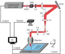
Femtosecond Laser Single-pass High Quality Direct Cutting Thin Quartz Glass Process Based on Filament Effect(Invited)
Kai LIAO, Wenjun WANG, Xuesong MEI, and Bin LIU
A one-step direct cutting method of 200 μm quartz glass using high-repetition frequency femtosecond laser combined with scanning galvanometer based on filament effect was proposed. Through the optimization of the processing process parameters, the fast and high-quality cutting of thin quartz glass is realized. The processing speed can be achieved 10 mm/s, the edge chipping is less 7.5 μm, and the roughness of the cross section is achieved 1 μm. The method realizes the simultaneous improvement of thin glass cutting efficiency and quality, and has a good application prospect in the field of laser processing. A one-step direct cutting method of 200 μm quartz glass using high-repetition frequency femtosecond laser combined with scanning galvanometer based on filament effect was proposed. Through the optimization of the processing process parameters, the fast and high-quality cutting of thin quartz glass is realized. The processing speed can be achieved 10 mm/s, the edge chipping is less 7.5 μm, and the roughness of the cross section is achieved 1 μm. The method realizes the simultaneous improvement of thin glass cutting efficiency and quality, and has a good application prospect in the field of laser processing.
Acta Photonica Sinica
- Publication Date: Jun. 25, 2021
- Vol. 50, Issue 6, 3 (2021)
Advances in the Preparation of Functional Surfaces with Special Wettability by Femtosecond Laser Ablation(Invited)
Sizhu WU, Xiaodong LÜ, Chuanzong LI, Chenchu ZHANG, Jianquan LI, Yi XIAO, and Dong WU
Functional surfaces with special wettability have played an important role in society and our daily life. Meanwhile, femtosecond laser has become an important tool to prepare a special wetting surface because of its unique manufacturing advantages. This article discusses the method of fabricating various microstructures by femtosecond laser, that is based on the connection between biological surface microstructures in nature and their practical applications. Then, three aspects of the preparation of the surface with special wettability via femtosecond laser are reviewed which are the “Janus” surfaces, the smart response surperhydrophobic surfaces, and the slippery surfaces. By summarizing the research results of the surface with special wettability prepared by femtosecond laser, this review provides a reference for the research, application, and future research direction of special wetting surfaces using a femtosecond laser. Functional surfaces with special wettability have played an important role in society and our daily life. Meanwhile, femtosecond laser has become an important tool to prepare a special wetting surface because of its unique manufacturing advantages. This article discusses the method of fabricating various microstructures by femtosecond laser, that is based on the connection between biological surface microstructures in nature and their practical applications. Then, three aspects of the preparation of the surface with special wettability via femtosecond laser are reviewed which are the “Janus” surfaces, the smart response surperhydrophobic surfaces, and the slippery surfaces. By summarizing the research results of the surface with special wettability prepared by femtosecond laser, this review provides a reference for the research, application, and future research direction of special wetting surfaces using a femtosecond laser.
Acta Photonica Sinica
- Publication Date: Jun. 25, 2021
- Vol. 50, Issue 6, 15 (2021)
Short-pulse Laser-induced Plasma Micro-etching of High-temperature and High Pressure Single Crystal Diamond
Xizhao LU, Jialin CHEN, Qiuling WEN, Jing LU, and Feng JIANG
A short-pulse (<200 ns) infrared (1 064 nm) Laser Induced Plasma Assisted Ablation (LIPAA) is considered as a micro-processing technology to ablate a single crystal diamond. The mechanism of different infrared laser parameters which include laser fluence, pulse width, repetition rate etc. influence on the micro-structure linewidth and depth was explored as well as the distance between single crystal diamond and copper target. While the pulse width is greater than 4 ns, the laser interacted on the good crystal orientation of the single crystal diamond with the prominent photothermal effect, and the laser fluence of the induced metal plasma cluster reaches a certain threshold, combined with the short pulse laser energy action, the surface temperature of the single crystal diamond rises rapidly to 600°C and above. At this time, the diamond surface layer has an etched micro-structure. When the laser with a pulse width of less than 4 ns bombards the surface of the target, the short-pulse laser bombards the target to induce metal plasma clusters. At this time, back sputtering of related metal targets and back etching and graphitization can also be achieved. The metal deposition and groove profiles are impacted on the pulse width and repetition rate of infrared laser. The experimental results prove that LIPAA is a new and reliable diamond micro-structure processing technology. A short-pulse (<200 ns) infrared (1 064 nm) Laser Induced Plasma Assisted Ablation (LIPAA) is considered as a micro-processing technology to ablate a single crystal diamond. The mechanism of different infrared laser parameters which include laser fluence, pulse width, repetition rate etc. influence on the micro-structure linewidth and depth was explored as well as the distance between single crystal diamond and copper target. While the pulse width is greater than 4 ns, the laser interacted on the good crystal orientation of the single crystal diamond with the prominent photothermal effect, and the laser fluence of the induced metal plasma cluster reaches a certain threshold, combined with the short pulse laser energy action, the surface temperature of the single crystal diamond rises rapidly to 600°C and above. At this time, the diamond surface layer has an etched micro-structure. When the laser with a pulse width of less than 4 ns bombards the surface of the target, the short-pulse laser bombards the target to induce metal plasma clusters. At this time, back sputtering of related metal targets and back etching and graphitization can also be achieved. The metal deposition and groove profiles are impacted on the pulse width and repetition rate of infrared laser. The experimental results prove that LIPAA is a new and reliable diamond micro-structure processing technology.
Acta Photonica Sinica
- Publication Date: Jun. 25, 2021
- Vol. 50, Issue 6, 129 (2021)
Topics
© Copyright 2018-2021 | Chinese Laser Press. All Rights Reserved 沪ICP备15018463号-20